- Sat. Apr 20th, 2024
Latest Post
 Revolutionizing College Football: NCAA’s New Technology Rules and Safety Measures
 Escanaba Entrepreneur Katelyn Beaver Receives $10,000 Grant to Expand Her Hand-Made Fishing Lure Business
 Get ready for a sensory-rich adventure with Disney’s new ‘Smellephants on Parade’ installation!
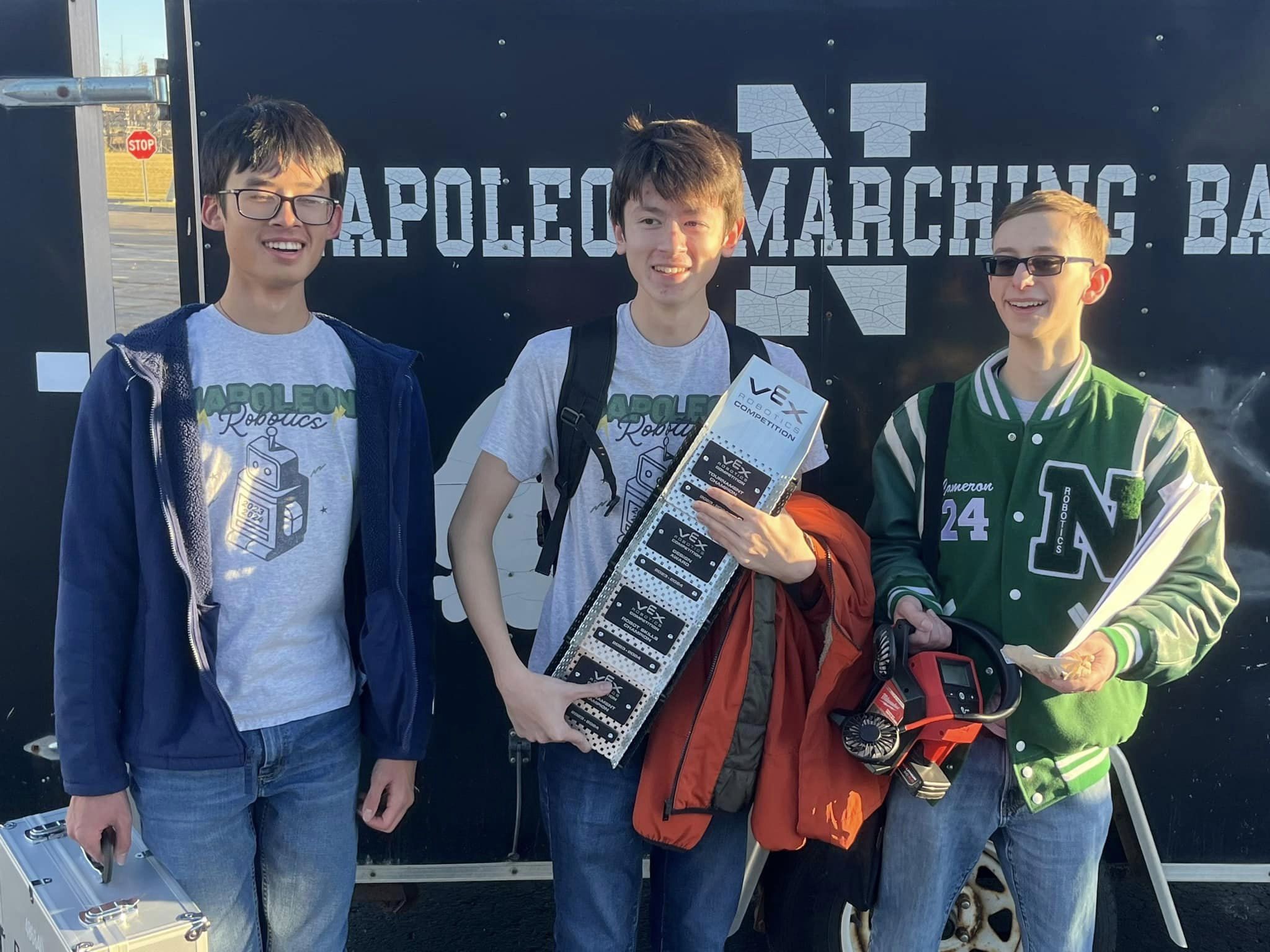 Napoleon High School’s Robotics Team Triple Triangularity Prepares for Second Consecutive VEX HS World Championship
 Experience Luxury and Unique Escapes at Travel + Leisure’s Top New England Hotels for 2024
Revolutionizing College Football: NCAA’s New Technology Rules and Safety Measures
The NCAA Football Rules Committee has approved new technology rules for college football, including the implementation of a two-minute warning in all levels of play. Similar to the NFL, automatic…
Escanaba Entrepreneur Katelyn Beaver Receives $10,000 Grant to Expand Her Hand-Made Fishing Lure Business
Katelyn Beaver, founder of Beavers Lures, a unique hand-made fishing lure business based in Escanaba, has received a $10,000 grant from the Federal Home Loan Bank of Indianapolis (FHLBI) Elevate…
Get ready for a sensory-rich adventure with Disney’s new ‘Smellephants on Parade’ installation!
The Magic Kingdom is set to receive a new sensory experience in May with the launch of “Smellephants on Parade” presented by Scentsy. The installation will be located in the…
Napoleon High School’s Robotics Team Triple Triangularity Prepares for Second Consecutive VEX HS World Championship
The Napoleon High School Robotics Team, Triple Triangularity, is set to compete in the VEX HS World Championship, scheduled for April 24-27 in Dallas, Texas. This year marks the second…
Experience Luxury and Unique Escapes at Travel + Leisure’s Top New England Hotels for 2024
Discover the world’s most exciting new hotels with Travel + Leisure’s 19th annual It List for 2024. This list features four properties in New England, including Faraway Martha’s Vineyard, Raffles…
Israel Strikes Iran: Tensions Escalate in Middle East as Blinken Calls for Calm
New tensions have emerged in the Middle East following reports of an Israeli strike on Iran. US Secretary of State Antony Blinken has urged for calm and de-escalation in the…
FINA Bans Chilean Aquatic Official for Misappropriating Funds: A Review of Recent Disciplinary Actions in Swimming and Diving
The Chilean Federation of Aquatics Sport’s former president, Marcos Jara, has been issued a 20-year ban by the Aquatics Integrity Unit of World Aquatics. This punishment was handed down after…
Libertarians, Big Tobacco: Smoking Restrictions Aren’t Personal Choices, They’re Public Health Imperatives
In recent years, the debate surrounding the merits of smoking restrictions has become increasingly clear-cut. While libertarians may argue against government intervention in personal choices, the overwhelming evidence supports the…
Biden’s Visit to Union Conference: Rebuilding Coalitions and Taking on the Wealthy.
The International Brotherhood of Electrical Workers held a conference, and President Biden took the opportunity to speak about his upbringing compared to that of his opponent. He highlighted how some…
Fragmented Global Economy: How Central Banks Can Adapt to Navigate Inflation Shocks and Maintain Economic Stability
Catherine Mann, a policymaker at the Bank of England, has raised concerns about the fragmentation of the global economy and its potential impact on inflation shocks in the future. She…